![]()
![]()
![]()
![]()
![]()
![]()
![]() Updated in
Updated in ![]() 2026 :
2026 : ![]() 5 :
5 : ![]() 20 : Materials AND circuits ;
20 : Materials AND circuits ;
(![]() Material,
Material,
![]() Material,
Material,
![]() Material,
Material,
![]() Material) ... ;
Material) ... ;
。
since May 2026, Gas-Solid Hydride Ion Battery, also see: structural Battery ... ;
。
(Content.Internet,
this DOMAIN,
USB-C)
Gene Therapy System : mineral "Materials" e.g.
Calcium ... ;
(Content.Internet,
this DOMAIN,
USB-C)
Gene Therapy System : mineral "Materials" e.g.
Iron ... ;
(Content.Internet,
this DOMAIN,
USB-C)
Gene Therapy System : mineral "Materials" e.g.
Magnesium ... ;
(Content.Internet,
this DOMAIN,
USB-C)
Gene Therapy System : mineral "Materials" e.g.
Potassium ... ;
(Content.Internet,
this DOMAIN,
USB-C)
Gene Therapy System : mineral "Materials" e.g.
Sodium ... ;
(Content.Internet,
this DOMAIN,
USB-C)
Gene Therapy
System : mineral "Materials" e.g. Vitamin ... ;
。
2025; (Antimony, Gallium, Germanium) ... ;
(51, Antimony, S b, 121.7),
(31, Gallium, G a, 69.7),
(32, Germanium, G e, 72.6),
also see: Chemical _Elements ... ;
。
2024; a new Graphene material (potentials in diff
color codes (iroLED); Usage (graphene), derived from
"graphite," doko
![]() WHERE single
atom layer of (6, Carbon,
C)
atoms;
WHERE single
atom layer of (6, Carbon,
C)
atoms;
。
2565;
2022; Model;
![]() micro SD;
micro SD;
。
2020 Modelled
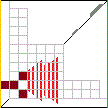 Magnetic Field Tesla (
![]() M F T, doko
M F T, doko
![]() WHERE "Red"
are) ... ; "Green" is R X X (Resistance X X); "Yellow" is R X Y (Resistance X Y);
depending upon material (e.g.
A I N,
G a A s,
G a N,
G e,
H g C d T e,
I n A s,
I n P,
metal oxide,
organic conductor,
S i,
S i C,
S i G e)
used,
WHERE "Red"
are) ... ; "Green" is R X X (Resistance X X); "Yellow" is R X Y (Resistance X Y);
depending upon material (e.g.
A I N,
G a A s,
G a N,
G e,
H g C d T e,
I n A s,
I n P,
metal oxide,
organic conductor,
S i,
S i C,
S i G e)
used,
![]() M F T 's (Val, Ref) may vary, so "Red" may vary, so called "Magnet Field Tesla";
Also see: Magnet;
3mComputer;
PHYSICS;
z G T S U;
M F T 's (Val, Ref) may vary, so "Red" may vary, so called "Magnet Field Tesla";
Also see: Magnet;
3mComputer;
PHYSICS;
z G T S U;
well trained kids! replied: WHY
you didn't define "Magnetic Field Tesla" as a schematic symbol sir ?
I wrote: don't you notice THAT "Red" ones are in parallel, it means "heat" and
we don't need heat that much for basic understanding of WHAT is M F T, therefore I
did not define IT inside of schematic;
Before testing and engineering materials, dual band transmitter should be understood basically.
Solid-state physics makes circuits analysis and design, computer science makes how to exploit thoroughly and how to deploy scientifically, YIN YANG of chemical properties and physical properties make new nano products ...;
。
Al-Cu vs. Cu: Al-Cu
and Cu in laminated metal film [2~3 layers] is design in comb electrode
structure which can perform antenna duplexer [Also see:
Fujitsu's SAW filter, SAW resonator];
A m p e r i u m wire,
superconducting ... , with
zero resistance (conduct
> 100 times) 285
A 66
copper wire; (antimony,
stibnite,
sulfur,
... ) also see: under sea, WHERE nearby underwater volcano (water)
IFF excluding water, hyper dimensional
![]() lights
... ; (Array
(C M O S gate-array) (B G A) (F P G A)
(P G A) (...) [some arrays are in
packaging
techniques]);
A S I C;
lights
... ; (Array
(C M O S gate-array) (B G A) (F P G A)
(P G A) (...) [some arrays are in
packaging
techniques]);
A S I C;
B i C MOS, Bipolar C MOS;
C CP, Chip Carrier Packages;
Characteristics in
1D, 2D,
3D, 4D, ... where information flows how;
C MOS![]() ;
C MP, Chemical Mechanical Polishing;
C NT, Carbon Nanotube [C60;
NEC laboratories' Dr.
S u m i o I i j i ma; 1991];
;
C MP, Chemical Mechanical Polishing;
C NT, Carbon Nanotube [C60;
NEC laboratories' Dr.
S u m i o I i j i ma; 1991];
(Design Rules (Active area rule) (Contact rule) (Distance constraint rule [dB heterodyned overlapped EM energy engineering]) (Electric arc rule) (Layout-design rule (Lambda rule) (Micron rule)) (Mass energy / A, B, C, D, ... , tree rule) (Metal rule) (Non-arc circumference rule [Wireless/Satellite engineering]) (Poly-Si rule) (Tangent line to non-arc circumference rule [Advanced optical engineering]) (...)); (Digital Circuits (Dynamic circuits (Domino logic circuits) (NORA logic circuits) (TS PC logic circuits) (...)) (Static circuits (Classical C MOS) (CV SL circuits) (Transmission-gate circuits) (...)) (...)); DIP [In common, max. pin count <=64]; DR C, Design Rule Check; DS P;
EOS, Electrical overstress; E SD, Electrostatic discharge;
FE T [Also see: FE T in Transistor]; FOX, Field Oxide; (FP GA (C LB) (I/O buffer) (Interconnection/structural programmable) (...)); FS M, Finite State Machines [Automata theory]; (Full adder (3 input (a) (b) (c)) (2 output (sum out) (carry out)) (...));
GA, Gate Array; G a As, Gallium Arsenide; G a As ME SF ET; Gallium nitride substrates [Also see: F PC]; Geometrical seems like physical but geometrical is not physical;
Holey fiber [Also see: Sumitomo];
I/O, Input/Output; In G a As, laser photo diodes; (Integration (U L SI) (V L SI) (...));
(Lithography (E beam![]() )
(...)); LOCOS;
)
(...)); LOCOS;
Mask; M CM, Multi Chip Modules;
Mercury Thallium Barium Calcium Copper Oxide, a substance for high temperature
superconducting
[Pg. 13, Force Fields, PHYSICS OF THE IMPOSSIBLE, M i c h i o K a k u, 2008];
Me so porous materials, structured/uniformed porous materials between 2 ~ 50 nm
Canon's usage;
(Metal (Al) (G ND) (Metal-1) (Metal-2![]() )
(VD D) (...)); Metal nano powder;
M MIC; MOS, Metal Oxide Semiconductor;
(MOS structure (Metal gate electrode) (Insulating oxide layer [i.e. SiO2])
(Substrate) (...));
MOS transistor;
MOS F ET; MOS IS, MOS Implementation
System;
MUX;
)
(VD D) (...)); Metal nano powder;
M MIC; MOS, Metal Oxide Semiconductor;
(MOS structure (Metal gate electrode) (Insulating oxide layer [i.e. SiO2])
(Substrate) (...));
MOS transistor;
MOS F ET; MOS IS, MOS Implementation
System;
MUX;
。
Materials in 2011, periodic table's malleable, magnetic, reactive, reflective, ... expensive materials are 21 Scandium Sc, 39 Yttrium Y, 57 Lanthanum La, 58 Cerium C e, 59 Praseodymium Pr, 60 Neodymium N d, 61 Promethium Pm, 62 Samarium S m, 63 Europium E u, 64 Gadolinium G d, 65 Terbium Tb, 66 Dysprosium D y, 67 Holmium Ho, 68 Erbium E r, 69 Thulium Tm, 70 Ytterbium Y b, and 71 Lutetium Lu; 2011 June, National Geographic; also see: 7mComputer;
。
n+; n MOS, n channel MOS;
Optical computing: M CP to Pixel to A P D;
p+; (Packaging (C CP, Chip Carrier Packages) (DIP) (M CM, Multi-Chip Modules) (PG A) (Q FP, Quad Flat Packs) (...)); PCB; PDA; Periodic Table; Photonic crystals; (Photo resist (negative photo-resist) (positive photo-resist) (...)); Physical and materials constant; PIE, Proton Induced Exfoliation, 11 slight 11 ♯ ♯ micro n s, i.e. flexible and thin wafer s; Pin pointing technique; P LA; p MOS, p channel MOS; poly-si [Also see: Poly-Si in Transistor]; PT H;
Q FP, Quad Flat Packs;
RAM; RPT, Repeated Transistors [Also see: non-repeatable transistors];
(Schematic (Draft level) (Gate level) (Transistor level) (...)); S EM, Scanning Electron Microscope; Si substrate; Si3N4; SiO2; S MT; (Substrate (Si) (...) ); superconductor magnets to levitate nonmagnetic materials i.e. d i a magnets and paramagnets; Swapping with 2 integer variables;
Timing diagram [i.e. Based on clock CL K, V DD can be classified into BL & BL, CS L, D IO & D IO, DL & DL, PS AE, W L, ... , thus SRAM can be monitored] where top notch pin level computer systems security becomes available; TiO2, Titanium dioxide's resistance changes WHEN and WHERE O2 exists, also see: O2 sensor; TS PC;
UV, one of the particles of light;
VD SM; VLSI design flow (Y-Chart = Algorithm [Behavioral] to Processor [Structural] to Chip floor plan [Geometrical] to Finite state machine [Behavioral] to Register A LU [Structural] to Module placement [Geometrical] to Module description [Behavioral] to Leaf cell [Structural] to Cell placement [Geometrical] to Boolean logical equation [Behavioral] to Transistor [Structural] to Mask [Geometrical]);
W/L ratio![]() ;
;
(Yield (Chip-yield) (Functional-yield) (Parametric-yield) (...));
...
|
|
|
|
|
|