![]() ;
; ![]() ;
;
![]() ; Updated in
2563 : on
; Updated in
2563 : on
![]() 2020 :
2020 :
![]() 8 :
8 :
![]() 6 :
Physics Law 137 ;
6 :
Physics Law 137 ;
![]()
![]()
![]()
![]()
![]()
![]() (law
137) :
remote (chip,
chipset, key) NFC;
(law
137) :
remote (chip,
chipset, key) NFC;
IoT must obey
![]() NFC3;
NFC3;
![]() NFC2;
NFC2;
![]() NFC1;
NFC,
Near Field Communication;
NFC1;
NFC,
Near Field Communication;
![]() NFC4, Near Field Communication 4; Also
see:
Electricity Power Plug;
IoT;
Remark: Hex={51,51,51} i.e. (Custom Color (Blue 81, Green 81, Red 81); custom
color (Hue 160, Lum 76, Sat 0)) ;
NFC4, Near Field Communication 4; Also
see:
Electricity Power Plug;
IoT;
Remark: Hex={51,51,51} i.e. (Custom Color (Blue 81, Green 81, Red 81); custom
color (Hue 160, Lum 76, Sat 0)) ;
![]() NFC;
NFC;
![]() NFC;
NFC;
![]() NFC;
NFC;
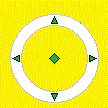
I wrote : WHEN I was doing construction (e.g. remodeling houses), one of my friends took a chip out of his car's key, and he kept a very tiny chip (approx. 2-3 mm in size) only and his car key could be anywhere but without the chip no one could start the engine;
well trained kids! replied : i.e. Location Awareness Response sir;
I wrote :
![]() HOW could that
be, regarding (approx. 2-3 mm in size) very tiny chip, without electrical
power, without connecting to any circuit, and it (the very tiny chip) must be
located next to the key, then OK to start the engine; IFF green, we've already
realized and understood Physics Law 136,
directional green,
doko
HOW could that
be, regarding (approx. 2-3 mm in size) very tiny chip, without electrical
power, without connecting to any circuit, and it (the very tiny chip) must be
located next to the key, then OK to start the engine; IFF green, we've already
realized and understood Physics Law 136,
directional green,
doko ![]() WHERE gravity spot indicator will be at the left ZCS of the DEE Box, so (open
directional, open environmental,
open structural) should be defined by one word e.g.
remote;
since we've learnt SQRT2 design model's floating points,
remote would be 100, among Engineering Notation of (10, 100, 1000, 10000,
100000, ... );
SQRT3 design model is NOT available to public;
WHERE gravity spot indicator will be at the left ZCS of the DEE Box, so (open
directional, open environmental,
open structural) should be defined by one word e.g.
remote;
since we've learnt SQRT2 design model's floating points,
remote would be 100, among Engineering Notation of (10, 100, 1000, 10000,
100000, ... );
SQRT3 design model is NOT available to public;
well trained kids! replied : very interesting sir, can you teach us more please e.g. (multi colors, multi time lines) for billions of devices HOW ?
I wrote : OK.
time constraint must be limited within (1 second, 2 second) Real-time, also see: -time; think that we human beings can survive for more than 300+ years, if compare to biological worms survive for a few hours;
space constraint must be
related to
![]() NFC,
Near Field Communication;
NFC,
Near Field Communication;
![]() kyori Distance
kyori Distance
![]() kyori Distance
kyori Distance
![]() kyori Distance;
Also see:
Distance;
kyori Distance;
Also see:
Distance;
think that
(multi colors,
multi time lines)
for billions
of
![]() devices;
devices;
action of my gift picture would be :
1st. before starting NFC chip design
model, we need to be refreshing with
this DOMAIN 's common
Schematic Symbols, e.g.
(![]() Analog Resonance,
Analog Resonance,
![]() coil,
coil,
 DEE Handle3,
 DEE _Jitter _Adjustment X,
![]() dual _band _transmitter,
dual _band _transmitter,
![]() E pi _cycles,
E pi _cycles,
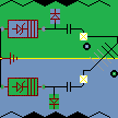 Gravity Harvest Power Antenna,
![]() jumper9 _f _MUX,
jumper9 _f _MUX,
![]() Latch1,
Latch1,
![]() Memristor _without _hole-board,
Memristor _without _hole-board,
![]() PINCH,
PINCH,
![]() ZOOM, ... ) ;
ZOOM, ... ) ;
2nd. before starting NFC chip design
model, we need to be refreshing with
this DOMAIN 's common
Schematic
Dimensional, e.g. (![]() 1 String 1 Hole Cause Green Structural Because Of Salt,
1 String 1 Hole Cause Green Structural Because Of Salt,
 28-108_beyond_DEE_mouth,
 AnotherWayToDefine1WayDEE,
 C Sequence Number Natural Cell Path Battery,
![]() DEE FMD _Our Earth,
DEE FMD _Our Earth,
 dubbing 2 or more ZCS holes
as heart beats,
dubbing 2 or more ZCS holes
as heart beats,
![]() EBEML,
EBEML,
 Light Speed Measurement,
 Yellow Background Based Green String Cell Path,
 ZCS_hole, ... ) ;
3rd. after understanding 1st (Schematic
Symbols) and 2nd (Schematic Dimensional), my
gift picture would be 2 EMI's Middle Path (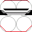 2EMIMP), 108x108 dimensional,
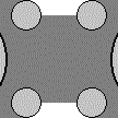
![]() And Then, 2 edges (bottom, top) must be your own
defined color codes and the 2 edges should not be the same color; for basic
understanding, this DOMAIN is using Maroon color at the top, Red color at the
bottom, and 4 circles equally within 108x108 dimensional;
And Then, 2 edges (bottom, top) must be your own
defined color codes and the 2 edges should not be the same color; for basic
understanding, this DOMAIN is using Maroon color at the top, Red color at the
bottom, and 4 circles equally within 108x108 dimensional;
for well trained kids!, color yourself
e.g. Green color at the top, Aqua color at the bottom;
for well trained kids!, color yourself e.g. Navy color at the top, Blue color at
the bottom;
i.e.
![]() HOW to design
model (NFC) very tiny chip is without electrical power, without connecting to
any circuit, ... ; because, regarding my gift picture
2EMIMP, that (approx. 2-3 mm in size) very tiny chip must obey Yellow
color, as Middle Path 's 2 EMI indicator or sensor, i.e. HOW NFC basic design
model is ... ; if you like to try IT yourself by applying polarization to the
Middle Path, regarding chip design, wafer design, also see:
Optics;
HOW to design
model (NFC) very tiny chip is without electrical power, without connecting to
any circuit, ... ; because, regarding my gift picture
2EMIMP, that (approx. 2-3 mm in size) very tiny chip must obey Yellow
color, as Middle Path 's 2 EMI indicator or sensor, i.e. HOW NFC basic design
model is ... ; if you like to try IT yourself by applying polarization to the
Middle Path, regarding chip design, wafer design, also see:
Optics;
Remark: regarding setsudo Perturbation, deviation of the defined system, if you define at the top, then bottom should be sensor, then if sensor prompts correct result, Middle Path should be your action (indicator) so you can bypass the defined (chip, chipset, key) i.e. reversed engineering;
|
|
|
|
|
|